
SKYSPIN
A digital computer with one microprocessor which acts as a CPU is called microcomputer.
It is a programmable, multipurpose, clock -driven, register-based electronic device that reads binary instructions from a storage device called memory, accepts binary data as input and processes data according to those instructions and provides results as output.
The microprocessor contains millions of tiny components like transistors, registers, and diodes that work together.
 A microprocessor consists of an ALU, control unit and register array. Where ALU
performs arithmetic and logical operations on the data received from an
input device or memory. Control unit controls the instructions and flow
of data within the computer. And, register array consists of registers identified by letters like B, C, D, E, H, L, and accumulator.
A microprocessor consists of an ALU, control unit and register array. Where ALU
performs arithmetic and logical operations on the data received from an
input device or memory. Control unit controls the instructions and flow
of data within the computer. And, register array consists of registers identified by letters like B, C, D, E, H, L, and accumulator.
It was a processor on a single chip. It could perform simple arithmetic and logical operations such as addition, subtraction, Boolean OR and Boolean AND.
I had a control unit capable of performing control functions like fetching an instruction from storage memory, decoding it, and then generating control pulses to execute it.
Other improved 64-bit processors are Celeron, Dual, Quad, Octa Core processors.
Instruction Set - The group of commands that the microprocessor can understand is called Instruction set. It is an interface between hardware and software.
Bus - Set of conductors intended to transmit data, address or control information to different elements in a microprocessor. A microprocessor will have three types of buses, i.e., data bus, address bus, and control bus.
IPC (Instructions Per Cycle) - It is a measure of how many instructions a CPU is capable of executing in a single clock.
Clock Speed - It is the number of operations per second the processor can perform. It can be expressed in megahertz (MHz) or gigahertz (GHz). It is also called the Clock Rate.
Bandwidth - The number of bits processed in a single instruction is called Bandwidth.
Word Length - The number of bits the processor can process at a time is called the word length of the processor. 8-bit Microprocessor may process 8 -bit data at a time. The range of word length is from 4 bits to 64 bits depending upon the type of the microcomputer.
Data Types - The microprocessor supports multiple data type formats like binary, ASCII, signed and unsigned numbers.
Initially, the instructions are stored in the storage memory of the computer in sequential order. The microprocessor fetches those instructions from the stored area (memory), then decodes it and executes those instructions till STOP instruction is met. Then, it sends the result in binary form to the output port. Between these processes, the register stores the temporary data and ALU (Arithmetic and Logic Unit) performs the computing functions.
Types of microprocessors:
Complex instruction set microprocessor –
The processors are designed to minimise the number of instructions per program and ignore the number of cycles per instructions. The compiler is used to translate a high level language to assembly level language because the length of code is relatively short and an extra RAM is used to store the instructions. These processors can do tasks like downloading, uploading and recalling data from memory. Apart from these tasks these microprocessor can perform complex mathematical calculation in a single command.
Example: IBM 370/168, VAX 11/780

It has following configuration:
The below diagram shows the block diagram of Intel 8085:

A flag is a flip-flop which indicates some conditions which arises after the execution of an arithmetic or logical instruction.
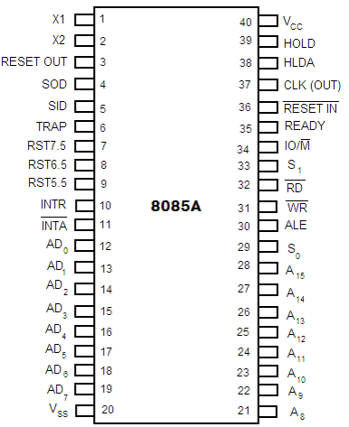 Fig: Pin diagram of Intel 8085 microprocessor
The descriptions of various pins are as follows:
Address Bus and Data Bus


RST 7.5, RST 6.5 and RST 5.5 are the restart interrupts which cause an internal restart to be automatically inserted.
The TRAP has the highest priority among interrupts. The order of priority of interrupts is as follows:
Vcc : +5 Vlots supply
Vss : ground reference
The 1st part of an instruction which specifies the task to be performed by the computer is called Opcode.
The 2nd part of the instruction is the data to be operated on, and it is called Operand. The Operand (or data) given in the instruction may be in various forms such as 8-bit or 16-bit data, 8-bit or 16-bit address, internal registers or a register or memory location.
According to the word size, the Intel 8085 instructions are classified into the following three types:
2. Two-byte instruction: In a two byte instruction the first byte of the instruction is its opcode and the second byte is either data or address.
Example:
MVI B, 05; 05 moved to register B.
06, 05; MVI B, 05 is in the code form.
The first byte 06 is the opcode for MVI B and second byte 05 is the data which is to be moved to register B.
3. Three-byte instruction: The first byte of the instruction is its opcode and the second and third bytes are either 16-bit data or 16-bit address.
Example:
LXI H, 2400H; Load H-L Pair with 2400H
21, 00, 24; LXI H, 2400H in the code form
The first byte 21 is the opcode for the instruction LXI H. The second 00 is 8 LSBs of the data (2400H), which is loaded into register L. The third byte 24 is 8 MSBs of the data (2400H), which is loaded into register H.
 The time required to fetch an instruction and necessary data from memory and to execute it, is called an instruction cycle. Or the total time required to execute an instruction is given by:

Where,

Timing Diagram for Instruction Cycle
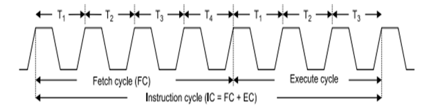
The whole operation of fetching an opcode takes three clock cycles. A slow memory may take more time.
If the operand is reside the general purpose registers, execution is immediately performed. The time taken in decoding and execution of an instruction is one clock cycle.
In some situations, an execute cycle may involve one or more read or write cycles or both.
Read Cycle: If an instruction contains data or operand address which are in the memory, the CPU has to perform some read operations to get the desired data. In case of a read cycle the instruction received from the memory are data or operand address instead of an opcode.
Write Cycle: In write cycle data are sent from the CPU to the memory or an output device.
One sub-division of an operation performed in one clock cycle is called a state or T-state. In short, one clock cycle of the system clock is referred to as a state.
RD (low active): If it is high or 1, then no data is read by the microprocessor. If signal is low or 0, then data is read by the microprocessor.
WR (low active): If it is high or 1, then no data is written by the microprocessor. If signal is low or 0, then data is written by the microprocessor.
IO/M (low active): A high or 1 on this signal indicates I/O operation while a low or 0 indicates memory operation.
S0, S1: S0 and S1 Indicate the type of machine cycle in progress.
The below table, shows the status of different control signal for different operation:
Example
STA 2400H: It stores the content of the accumulator in the memory location 2400H.
32, 00, 24: The above instruction in the code form.
In this instruction, 2400H is the memory address where data is to be stored. It is given in the instruction itself. The 2nd and 3rd bytes of the instruction specify the address of the memory location. Here, it is understood that the source of the data is accumulator.
Example:
MOV A, B: Move the content of B register to register A.
78: The instruction in the code form.
In the above example, MOV A, B is 78H. Besides the operation to be performed the opcode also specifies source and destination registers.
The opcode 78H can be written in binary form as 01111000. The first two bits, i.e. 0 1 are for MOV operation, the next three bits 1 1 1 are the binary code for register A, and the last three bits 000 are the binary code for register B.
Example
Example
LXI H, 2500 is an example of immediate addressing. 2500 is 16-bit data which is given in the instruction itself. It is to be loaded into H-L pair.
Example
CMA, RAL, RAR, etc.
MOV A 2B (load 2BH in register A)
MOV B 39 (load 39H in register B)
ADD B (A = A + B)
These set of instructions will set the auxiliary carry flag to 1, as on adding 2B and 39, addition of lower order nibbles B and 9 will generate a carry.
4. Parity Flag (P) – If after any arithmetic or logical operation the result has even parity, an even number of 1 bits, the parity register becomes set i.e. 1, otherwise it becomes reset i.e. 0. 1-accumulator has even number of 1 bits
0-accumulator has odd parity
Example:
MVI A 05 (load 05H in register A)
This instruction will set the parity flag to 1 as the BCD code of 05H is 00000101, which contains even number of ones i.e. 2.
5. Carry Flag (CY) – Carry is generated when performing n bit operations and the result is more than n bits, then this flag becomes set i.e. 1, otherwise it becomes reset i.e. 0.
During subtraction (A-B), if A>B it becomes reset and if (A<B) it becomes set.
Carry flag is also called borrow flag. 1-carry out from MSB bit on addition or borrow into MSB bit on subtraction
0-no carry out or borrow into MSB bit
Example:
MVI A 30 (load 30H in register A)
MVI B 40 (load 40H in register B)
SUB B (A = A – B)
These set of instructions will set the carry flag to 1 as 30 – 40 generates a carry/borrow.
MVI A 40 (load 40H in register A)
MVI B 30 (load 30H in register B)
SUB B (A = A – B)
These set of instructions will reset the sign flag to 0 as 40 – 30 does not generate any carry/borrow.
UNIT-1 (CHAPTER-1 INTRODUCTION TO MICROPROCESSOR)
What is a Microprocessor?
Computer's Central Processing Unit (CPU) built on a single Integrated Circuit (IC) is called a microprocessor.A digital computer with one microprocessor which acts as a CPU is called microcomputer.
It is a programmable, multipurpose, clock -driven, register-based electronic device that reads binary instructions from a storage device called memory, accepts binary data as input and processes data according to those instructions and provides results as output.
The microprocessor contains millions of tiny components like transistors, registers, and diodes that work together.
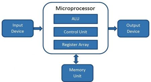
Block Diagram of a Microcomputer
A microprocessor consists of an ALU, control unit and register array. Where ALU
performs arithmetic and logical operations on the data received from an
input device or memory. Control unit controls the instructions and flow
of data within the computer. And, register array consists of registers identified by letters like B, C, D, E, H, L, and accumulator.Evolution of Microprocessors
We can categorize the microprocessor according to the generations or according to the size of the microprocessor:First Generation (4 - bit Microprocessors)
The first generation microprocessors were introduced in the year 1971-1972 by Intel Corporation. It was named Intel 4004 since it was a 4-bit processor.It was a processor on a single chip. It could perform simple arithmetic and logical operations such as addition, subtraction, Boolean OR and Boolean AND.
I had a control unit capable of performing control functions like fetching an instruction from storage memory, decoding it, and then generating control pulses to execute it.
Second Generation (8 - bit Microprocessor)
The second generation microprocessors were introduced in 1973 again by Intel. It was a first 8 - bit microprocessor which could perform arithmetic and logic operations on 8-bit words. It was Intel 8008, and another improved version was Intel 8088.Third Generation (16 - bit Microprocessor)
The third generation microprocessors, introduced in 1978 were represented by Intel's 8086, Zilog Z800 and 80286, which were 16 - bit processors with a performance like minicomputers.Fourth Generation (32 - bit Microprocessors)
Several different companies introduced the 32-bit microprocessors, but the most popular one is the Intel 80386.Fifth Generation (64 - bit Microprocessors)
From 1995 to now we are in the fifth generation. After 80856, Intel came out with a new processor namely Pentium processor followed by Pentium Pro CPU, which allows multiple CPUs in a single system to achieve multiprocessing.Other improved 64-bit processors are Celeron, Dual, Quad, Octa Core processors.
Basic Terms used in Microprocessor
Here is a list of some basic terms used in microprocessor:Instruction Set - The group of commands that the microprocessor can understand is called Instruction set. It is an interface between hardware and software.
Bus - Set of conductors intended to transmit data, address or control information to different elements in a microprocessor. A microprocessor will have three types of buses, i.e., data bus, address bus, and control bus.
IPC (Instructions Per Cycle) - It is a measure of how many instructions a CPU is capable of executing in a single clock.
Clock Speed - It is the number of operations per second the processor can perform. It can be expressed in megahertz (MHz) or gigahertz (GHz). It is also called the Clock Rate.
Bandwidth - The number of bits processed in a single instruction is called Bandwidth.
Word Length - The number of bits the processor can process at a time is called the word length of the processor. 8-bit Microprocessor may process 8 -bit data at a time. The range of word length is from 4 bits to 64 bits depending upon the type of the microcomputer.
Data Types - The microprocessor supports multiple data type formats like binary, ASCII, signed and unsigned numbers.
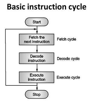
Working of Microprocessor
The microprocessor follows a sequence to execute the instruction: Fetch, Decode, and then Execute.Initially, the instructions are stored in the storage memory of the computer in sequential order. The microprocessor fetches those instructions from the stored area (memory), then decodes it and executes those instructions till STOP instruction is met. Then, it sends the result in binary form to the output port. Between these processes, the register stores the temporary data and ALU (Arithmetic and Logic Unit) performs the computing functions.
Features of Microprocessor
- Low Cost - Due to integrated circuit technology microprocessors are available at very low cost. It will reduce the cost of a computer system.
- High Speed - Due to the technology involved in it, the microprocessor can work at very high speed. It can execute millions of instructions per second.
- Small Size - A microprocessor is fabricated in a very less footprint due to very large scale and ultra large scale integration technology. Because of this, the size of the computer system is reduced.
- Versatile - The same chip can be used for several applications, therefore, microprocessors are versatile.
- Low Power Consumption - Microprocessors are using metal oxide semiconductor technology, which consumes less power.
- Less Heat Generation - Microprocessors uses semiconductor technology which will not emit much heat as compared to vacuum tube devices.
- Reliable - Since microprocessors use semiconductor technology, therefore, the failure rate is very less. Hence it is very reliable.
- Portable - Due to the small size and low power consumption microprocessors are portable.
Types of microprocessors:
Complex instruction set microprocessor –
The processors are designed to minimise the number of instructions per program and ignore the number of cycles per instructions. The compiler is used to translate a high level language to assembly level language because the length of code is relatively short and an extra RAM is used to store the instructions. These processors can do tasks like downloading, uploading and recalling data from memory. Apart from these tasks these microprocessor can perform complex mathematical calculation in a single command.
Example: IBM 370/168, VAX 11/780
- Reduced instruction set microprocessor –
These processor are made according to function. They are designed to reduce the execution time by using the simplified instruction set. They can carry out small things in specific commands. These processors complete commands at faster rate. They require only one clock cycle to implement a result at uniform execution time. There are number of registers and less number of transistors. To access the memory location LOAD and STORE instructions are used.
Example: Power PC 601, 604, 615, 620 - Super scalar microprocessor –
These processors can perform many tasks at a time. They can be used for ALUs and multiplier like array. They have multiple operation unit and perform tasts my executing multiple commands. - Application specific integrated circuit –
These processors are application specific like for personal digital assistant computers. They are designed according to proper specification. - Digital signal multiprocessor –
These processors are used to convert signals like analog to digital or digital to analog. The chips of these processors are used in many devices such as RADAR SONAR home theatres etc.
- High processing speed
- Compact size
- Easy maintenance
- Can perform complex mathematics
- Flexible
- Can be improved according to requirement
- Overheating occurs due to overuse
- Performance depends on size of data
- Large board size than microcontrollers
- Most microprocessors do not support floating point operations
Microprocessor Architecture
The microprocessor is the CPU (Central Processing Unit) of a computer. It is the heart of the computer. Here, we will describe Intel 8085 as it is one of the most popular 8-bit microprocessor.Intel 8085
Intel 8085 is an 8-bit, NMOS microprocessor designed by Intel in 1977.It has following configuration:
- It is a 40 pin I.C. package fabricated on a single LSI chip.
- The Intel 8085 uses a single +5Vd.c. supply for its operation.
- Intel 8085?s clock speed is about 3 MHz; the clock cycle is of 320ns.
- 8 ?bit data bus.
- Address bus is of 16-bit, which can address up to 64KB
- 16-bit stack pointer
- 16 bit PC (Program Counter)
- Six 8-bit registers are arranged in pairs :BC, DE, HL
The below diagram shows the block diagram of Intel 8085:
ALU
The Arithmetic and Logic Unit, ALU performs the arithmetic and logical operations:- Addition
- Subtraction
- Logical AND
- Logical OR
- Logical EXCLUSIVE OR
- Complement (Logical NOT)
- Increment (add 1)
- Decrement (subtract 1)
- Left shift, Rotate left, Rotate right
- Clear, etc.
Timing and Control Unit
The timing and control unit is the section of the CPU.- It is used to generate timing and control signals which are necessary for the execution of instructions.
- It is used to control data flow between CPU and peripherals (including memory).
- It is used to provide status, control and timing signals which are required for the operation of memory and I/O devices.
- It is used to control the entire operations of the microprocessor and peripherals connected to it.
Registers
Registers are used for temporary storage and manipulation of data and instructions by the microprocessor. Data remain in the registers till they are sent to the I/O devices or memory. Intel 8085 microprocessor has the following registers:- One 8-bit accumulator (ACC) i.e. register A
- Six general purpose registers of 8-bit, these are B,C, D, E, H and L
- One 16-bit stack pointer, SP
- One 16-bit Program Counter, PC
- Instruction register
- Temporary register
A flag is a flip-flop which indicates some conditions which arises after the execution of an arithmetic or logical instruction.
- Accumulator (ACC): The accumulator is an 8-bit
register associated with the ALU. The register 'A' is an accumulator in
the 8085. It is used to hold one of the operands of an arithmetic and
logical operation.
The final result of an arithmetic or logical operation is also placed in the accumulator. - General-Purpose Registers: The 8085 microprocessor contains six 8-bit general purpose registers. They are: B, D, C, E, H and L register.
To hold data of 16-bit a combination of two 8-bit registers can be employed.
The combination of two 8-bit registers is called register pair. The valid register pairs in the 8085 are: D-E, B-C and H-L. The H-L pair is used to act as a memory pointer. - Program Counter (PC): It is a 16-bit special
purpose register. It is used to hold the address of memory of the next
instruction to be executed. It keeps the track of the instruction in a
program while they are being executed.
The microprocessor increments the content of the next program counter during the execution of an instruction so that at the end of the execution of an instruction it points to the next instruction?s address in the program. - Stack Pointer (SP): It is a 16-bit special function
register used as memory pointer. A stack is nothing but a portion of
RAM. In the stack, the contents of only those registers are saved, which
are needed in the later part of the program.
The stack pointer (SP) controls the addressing of the stack. The Stack Pointer contains the address of the top element of data stored in the stack. - Instruction Register: The instruction register holds the opcode (operation code or instruction code) of the instruction which is being decoded and executed.
- Temporary Register: It is an 8-bit register associated with the ALU. It holds data during an arithmetic/logical operation. It is used by the microprocessor. It is not accessible to programmer.
- Flags: The Intel 8085 microprocessor contains five flip-flops to serve as a status flags. The flip-flops are reset or set according to the conditions which arise during an arithmetic or logical operation.
- Carry Flag (CS)
- Parity Flag (P)
- Auxiliary Carry Flag (AC)
- Zero Flag(Z)
- Sign Flag(S)
Data and Address Bus
- The Intel 8085 is an 8-bit microprocessor. Its data bus is 8-bit wide and therefore, 8 bits of data can be transmitted in parallel from or to the microprocessor.
- The Intel 8085 requires an address bus of 16-bit wide as the memory addresses are of 16-bits.
- The 8 most significant bits of the address are transmitted by the address bus, A-bus (pins A8 ? A15).
- The 8 least significant bits of the address are transmitted by data/address bus, AD-bus (pins AD0 ? AD7).
Pin Configuration
Fig: Pin diagram of Intel 8085 microprocessorThe descriptions of various pins are as follows:
Address Bus and Data Bus
- A8 ? A15 (Output): These are address bus and are used for the most significant bits of the memory address or 8-bits of I/O address.
- AD0 ? AD7 (Input/output): These are time multiplexed address/data bus i.e. they serve dual purpose. They are used for the least significant 8 bits of the memory address or I/O address during the first cycle. Again they are used for data during 2nd and 3rd clock cycles.
- ALE (Output): ALE stands for Address Latch Enable signal. ALE goes high during first clock cycle of a machine cycle and enables the lower 8-bits of the address to be latched either into the memory or external latch.
- IO/M (Output): It is a status signal which distinguishes whether the address is for memory or I/O device.
- S0, S1 (Output): These are status signals sent by the microprocessors to distinguish the various types of operation given in table below:
- RD (Output): RD is a signal to control READ operation. When it goes low, the selected I/O device or memory is read.
- WR (Output): WR is a signal to control WRITE operation. When it goes low, the data bus' data is written into the selected memory or I/O location.
- READY (Input): It is used by the microprocessor to sense whether a peripheral is ready to transfer a data or not. If READY is high, the peripheral is ready. If it is low the micro processor waits till it goes high.
- HOLD (INPUT): HOLD indicates that another device is requesting for the use of the address and data bus.
- HLDA (OUTPUT): HLDA is a signal for HOLD acknowledgement which indicates that the HOLD request has been received. After the removal of this request the HLDA goes low.
- INTR (Input): INTR is an Interrupt Request Signal. Among interrupts it has the lowest priority. The INTR is enabled or disabled by software.
- INTA (Output): INTA is an interrupt acknowledgement sent by the microprocessor after INTR is received.
- RST 5.5, 6.5, 7.5 and TRAP (Inputs): These all are interrupts. When any interrupt is recognized the next instruction is executed from a fixed location in the memory as given below:
RST 7.5, RST 6.5 and RST 5.5 are the restart interrupts which cause an internal restart to be automatically inserted.
The TRAP has the highest priority among interrupts. The order of priority of interrupts is as follows:
- TRAP (Highest priority)
- RST 7.5
- RST 6.5
- RST 5.5
- INTR (Lowest priority).
- RESET IN (Input): It resets the program counter (PC) to 0. It also resets interrupt enable and HLDA flip-flops. The CPU is held in reset condition till RESET is not applied.
- RESET OUT (Output): RESET OUT indicates that the CPU is being reset.
- X1, X2 (Input): X1 and X2 are terminals to be connected to an external crystal oscillator which drives an internal circuitry of the microprocessor. It is used to produce a suitable clock for the operation of microprocessor.
- CLK (Output): CLK is a clock output for user, which can be used for other digital ICs. Its frequency is same at which processor operates.
- SID (Input): SID is data line for serial input. The data on this line is loaded into the seventh bit of the accumulator when RIM instruction is executed.
- SOD (Output): SOD is a data line for serial output. The seventh bit of the accumulator is output on SOD line when SIM instruction is executed.
Vcc : +5 Vlots supply
Vss : ground reference
8085 Instructions
An instruction of computer is a command given to the computer to perform a specified operation on given data. Some instructions of Intel 8085 microprocessor are: MOV, MVI, LDA, STA, ADD, SUB, RAL, INR, MVI, etc.Opcode and Operands
Each instruction contains two parts: Opcode (Operation code) and Operand.The 1st part of an instruction which specifies the task to be performed by the computer is called Opcode.
The 2nd part of the instruction is the data to be operated on, and it is called Operand. The Operand (or data) given in the instruction may be in various forms such as 8-bit or 16-bit data, 8-bit or 16-bit address, internal registers or a register or memory location.
Instruction Word Size
A digital computer understands instruction written in binary codes (machine codes). The binary codes of all instructions are not of the same length.According to the word size, the Intel 8085 instructions are classified into the following three types:
- One byte instruction
- Two byte instruction
- Three byte instruction
- MOV A, B - Move the content of the register B to register A.
- ADD B ? Add the content of register B to the content of the accumulator.
2. Two-byte instruction: In a two byte instruction the first byte of the instruction is its opcode and the second byte is either data or address.
Example:
MVI B, 05; 05 moved to register B.
06, 05; MVI B, 05 is in the code form.
The first byte 06 is the opcode for MVI B and second byte 05 is the data which is to be moved to register B.
3. Three-byte instruction: The first byte of the instruction is its opcode and the second and third bytes are either 16-bit data or 16-bit address.
Example:
LXI H, 2400H; Load H-L Pair with 2400H
21, 00, 24; LXI H, 2400H in the code form
The first byte 21 is the opcode for the instruction LXI H. The second 00 is 8 LSBs of the data (2400H), which is loaded into register L. The third byte 24 is 8 MSBs of the data (2400H), which is loaded into register H.
Instruction Cycle
The time required to fetch an instruction and necessary data from memory and to execute it, is called an instruction cycle. Or the total time required to execute an instruction is given by:Where,
Timing Diagram for Instruction Cycle
- Fetch the instruction (Fetch Cycle)
The whole operation of fetching an opcode takes three clock cycles. A slow memory may take more time.
- Decode the instruction (Decode Cycle)
- Execute the Instruction (Execute Cycle)
If the operand is reside the general purpose registers, execution is immediately performed. The time taken in decoding and execution of an instruction is one clock cycle.
In some situations, an execute cycle may involve one or more read or write cycles or both.
Read Cycle: If an instruction contains data or operand address which are in the memory, the CPU has to perform some read operations to get the desired data. In case of a read cycle the instruction received from the memory are data or operand address instead of an opcode.
Write Cycle: In write cycle data are sent from the CPU to the memory or an output device.
- Machine Cycle and State
One sub-division of an operation performed in one clock cycle is called a state or T-state. In short, one clock cycle of the system clock is referred to as a state.
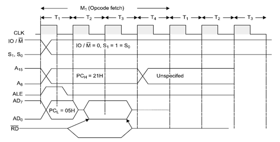
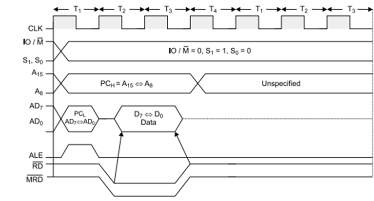
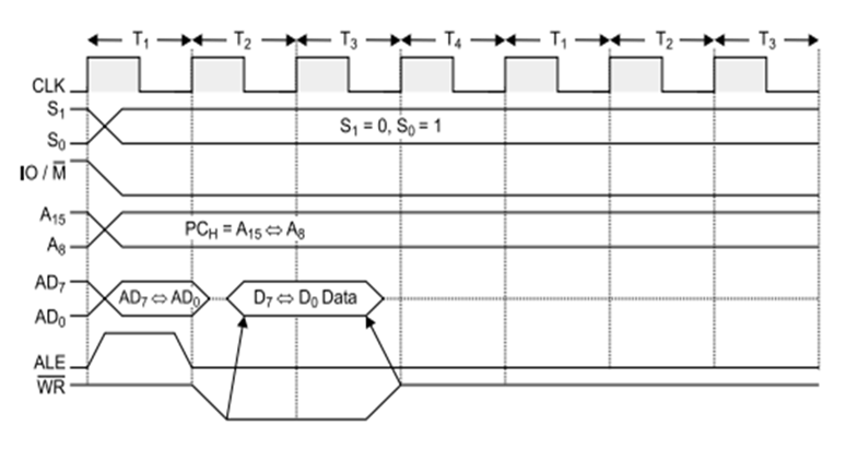
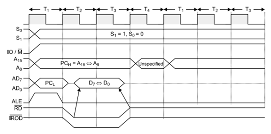
Timing Diagram
The necessary steps carried out in a machine cycle can be represented graphically. Such a graphical representation is called timing diagram. The timing diagram for opcode fetch, memory read, memory write, I/O read and I/O write will be discussed below:- Timing Diagram for Opcode Fetch Cycle:
- Timing Diagram for Memory Read
- Timing Diagram for Memory Write
- Timing Diagram for I/O Read
- Timing Diagram for I/O Write
In the above diagrams, the basic used parameters are:
ALE: ALE indicates the availability of a valid address on the multiplexed address/data lines. When it is high or 1, then it acts as an address bus and when low or 0, then it acts as a data bus.RD (low active): If it is high or 1, then no data is read by the microprocessor. If signal is low or 0, then data is read by the microprocessor.
WR (low active): If it is high or 1, then no data is written by the microprocessor. If signal is low or 0, then data is written by the microprocessor.
IO/M (low active): A high or 1 on this signal indicates I/O operation while a low or 0 indicates memory operation.
S0, S1: S0 and S1 Indicate the type of machine cycle in progress.
The below table, shows the status of different control signal for different operation:
Instruction Set of 8085
Instruction and Data Formats
The various techniques to specify data for instructions are:- 8-bit or 16-bit data may be directly given in the instruction itself.
- The address of the memory location, I/O port or I/O device, where data resides, may be given in the instruction itself.
- In some instructions, only one register is specified. The content of the specified register is one of the operands.
- Some instructions specify two registers. The contents of the registers are the required data.
- In some instructions, data is implied. The most instructions of this type operate on the content of the accumulator.
Addressing Modes
Each instruction requires some data on which it has to operate. There are different techniques to specify data for instructions. These techniques are called addressing modes. Intel 8085 uses the following addressing modes:- Direct Addressing
Example
STA 2400H: It stores the content of the accumulator in the memory location 2400H.
32, 00, 24: The above instruction in the code form.
In this instruction, 2400H is the memory address where data is to be stored. It is given in the instruction itself. The 2nd and 3rd bytes of the instruction specify the address of the memory location. Here, it is understood that the source of the data is accumulator.
- Register Addressing
Example:
MOV A, B: Move the content of B register to register A.
78: The instruction in the code form.
In the above example, MOV A, B is 78H. Besides the operation to be performed the opcode also specifies source and destination registers.
The opcode 78H can be written in binary form as 01111000. The first two bits, i.e. 0 1 are for MOV operation, the next three bits 1 1 1 are the binary code for register A, and the last three bits 000 are the binary code for register B.
- Register Indirect Addressing
Example
- LXI H, 2500 H - Load H-L pair with 2500H.
- MOV A, M - Move the content of the memory location, whose address is in H-L pair (i.e. 2500 H) to the accumulator.
- HLT - Halt.
- Immediate Addressing
Example
LXI H, 2500 is an example of immediate addressing. 2500 is 16-bit data which is given in the instruction itself. It is to be loaded into H-L pair.
- Implicit Addressing
Example
CMA, RAL, RAR, etc.
Status Flags
There is a set of five flip-flops which indicate status (condition) arising after the execution of arithmetic and logic instructions. These are:- Carry Flag (CS)
- Parity Flag (P)
- Auxiliary Carry Flags (AC)
- Zero Flags (Z)
- Sign Flags (S)
Flag register in 8085 microprocessor
The Flag register is a Special Purpose Register. Depending
upon the value of result after any arithmetic and logical operation the
flag bits become set (1) or reset (0). In 8085 microprocessor, flag
register consists of 8 bits and only 5 of them are useful.
The 5 flags are:- Sign Flag (S) – After any operation if the MSB
(B(7)) of the result is 1, it indicates the number is negative and the
sign flag becomes set, i.e. 1. If the MSB is 0, it indicates the number
is positive and the sign flag becomes reset i.e. 0.
from 00H to 7F, sign flag is 0
from 80H to FF, sign flag is 1 1- MSB is 1 (negative)
0- MSB is 0 (positive)
Example:
MVI A 30 (load 30H in register A)
MVI B 40 (load 40H in register B)
SUB B (A = A – B)
These set of instructions will set the sign flag to 1 as 30 – 40 is a negative number.
MVI A 40 (load 40H in register A)
MVI B 30 (load 30H in register B)
SUB B (A = A – B)
These set of instructions will reset the sign flag to 0 as 40 – 30 is a positive number.
- Zero Flag (Z) – After any arithmetical or logical
operation if the result is 0 (00)H, the zero flag becomes set i.e. 1,
otherwise it becomes reset i.e. 0.
00H zero flag is 1.
from 01H to FFH zero flag is 0 1- zero result
0- non-zero result
Example:
MVI A 10 (load 10H in register A)
SUB A (A = A – A)
These set of instructions will set the zero flag to 1 as 10H – 10H is 00H
- Auxiliary Carry Flag (AC) – This flag is used in
BCD number system(0-9). If after any arithmetic or logical operation
D(3) generates any carry and passes on to B(4) this flag becomes set
i.e. 1, otherwise it becomes reset i.e. 0. This is the only flag
register which is not accessible by the programmer
1-carry out from bit 3 on addition or borrow into bit 3 on subtraction
0-otherwise
MOV A 2B (load 2BH in register A)
MOV B 39 (load 39H in register B)
ADD B (A = A + B)
These set of instructions will set the auxiliary carry flag to 1, as on adding 2B and 39, addition of lower order nibbles B and 9 will generate a carry.
4. Parity Flag (P) – If after any arithmetic or logical operation the result has even parity, an even number of 1 bits, the parity register becomes set i.e. 1, otherwise it becomes reset i.e. 0. 1-accumulator has even number of 1 bits
0-accumulator has odd parity
Example:
MVI A 05 (load 05H in register A)
This instruction will set the parity flag to 1 as the BCD code of 05H is 00000101, which contains even number of ones i.e. 2.
5. Carry Flag (CY) – Carry is generated when performing n bit operations and the result is more than n bits, then this flag becomes set i.e. 1, otherwise it becomes reset i.e. 0.
During subtraction (A-B), if A>B it becomes reset and if (A<B) it becomes set.
Carry flag is also called borrow flag. 1-carry out from MSB bit on addition or borrow into MSB bit on subtraction
0-no carry out or borrow into MSB bit
Example:
MVI A 30 (load 30H in register A)
MVI B 40 (load 40H in register B)
SUB B (A = A – B)
These set of instructions will set the carry flag to 1 as 30 – 40 generates a carry/borrow.
MVI A 40 (load 40H in register A)
MVI B 30 (load 30H in register B)
SUB B (A = A – B)
These set of instructions will reset the sign flag to 0 as 40 – 30 does not generate any carry/borrow.


0 Comments