SKYSPIN
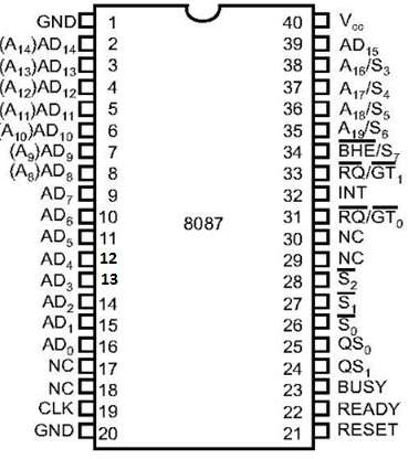
 The following list provides the Pin Description of 8087 −
 RQ/GT1 & RQ/GT0 − These are the Request/Grant signals used by the 8087 processors to gain control of the bus from the host processor 8086/8088 for operand transfers.
8087 Pin Description
Let us first take a look at the pin diagram of 8087 −
 The following list provides the Pin Description of 8087 −
- AD0 – AD15 − These are the time multiplexed address/data lines, which carry addresses during the first clock cycle and data from the second clock cycle onwards.
- A19 / S6 – A16/S − These lines are the time multiplexed address/status lines. It functions in a similar way to the corresponding pins of 8086. The S6, S4 and S3 are permanently high, while the S5 is permanently low.
- $\overline{BHE}$/S7 − During the first clock cycle, the $\overline{BHE}$/S7 is used to enable data on to the higher byte of the 8086 data bus and after that works as status line S7.
- QS1, QS0 − These are queue status
input signals which provides the status of instruction queue, their
conditions as shown in the following table −
- INT − It is an interrupt signal, which changes to high when an unmasked exception has been received during the execution.
- BUSY − It is an output signal, when it is high it indicates a busy state to the CPU.
- READY − It is an input signal used to inform the coprocessor whether the bus is ready to receive data or not.
- RESET − It is an input signal used to reject the internal activities of the coprocessor and prepare it for further execution whenever required by the CPU.
- CLK − The CLK input provides the basic timings for the processor operation.
- VCC − It is a power supply signal, which requires +5V supply for the operation of the circuit.
- S0, S1, S2 − These are the status signals that provide the status of the operation which is used by the Bus Controller 8087 to generate memory and I/O control signals. These signals are active during the fourth clock cycle.


0 Comments