SKYSPIN
It has following configuration:
The below diagram shows the block diagram of Intel 8085:

A flag is a flip-flop which indicates some conditions which arises after the execution of an arithmetic or logical instruction.
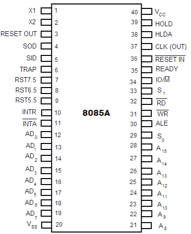
 Fig: Pin diagram of Intel 8085 microprocessor
The descriptions of various pins are as follows:
Address Bus and Data Bus


RST 7.5, RST 6.5 and RST 5.5 are the restart interrupts which cause an internal restart to be automatically inserted.
The TRAP has the highest priority among interrupts. The order of priority of interrupts is as follows:
Vcc : +5 Vlots supply
Vss : ground reference
Microprocessor Architecture
The microprocessor is the CPU (Central Processing Unit) of a computer. It is the heart of the computer. Here, we will describe Intel 8085 as it is one of the most popular 8-bit microprocessor.Intel 8085
Intel 8085 is an 8-bit, NMOS microprocessor designed by Intel in 1977.It has following configuration:
- It is a 40 pin I.C. package fabricated on a single LSI chip.
- The Intel 8085 uses a single +5Vd.c. supply for its operation.
- Intel 8085?s clock speed is about 3 MHz; the clock cycle is of 320ns.
- 8 ?bit data bus.
- Address bus is of 16-bit, which can address up to 64KB
- 16-bit stack pointer
- 16 bit PC (Program Counter)
- Six 8-bit registers are arranged in pairs :BC, DE, HL
The below diagram shows the block diagram of Intel 8085:

ALU
The Arithmetic and Logic Unit, ALU performs the arithmetic and logical operations:- Addition
- Subtraction
- Logical AND
- Logical OR
- Logical EXCLUSIVE OR
- Complement (Logical NOT)
- Increment (add 1)
- Decrement (subtract 1)
- Left shift, Rotate left, Rotate right
- Clear, etc.
Timing and Control Unit
The timing and control unit is the section of the CPU.- It is used to generate timing and control signals which are necessary for the execution of instructions.
- It is used to control data flow between CPU and peripherals (including memory).
- It is used to provide status, control and timing signals which are required for the operation of memory and I/O devices.
- It is used to control the entire operations of the microprocessor and peripherals connected to it.
Registers
Registers are used for temporary storage and manipulation of data and instructions by the microprocessor. Data remain in the registers till they are sent to the I/O devices or memory. Intel 8085 microprocessor has the following registers:- One 8-bit accumulator (ACC) i.e. register A
- Six general purpose registers of 8-bit, these are B,C, D, E, H and L
- One 16-bit stack pointer, SP
- One 16-bit Program Counter, PC
- Instruction register
- Temporary register
A flag is a flip-flop which indicates some conditions which arises after the execution of an arithmetic or logical instruction.
- Accumulator (ACC): The accumulator is an 8-bit
register associated with the ALU. The register 'A' is an accumulator in
the 8085. It is used to hold one of the operands of an arithmetic and
logical operation.
The final result of an arithmetic or logical operation is also placed in the accumulator. - General-Purpose Registers: The 8085 microprocessor contains six 8-bit general purpose registers. They are: B, D, C, E, H and L register.
To hold data of 16-bit a combination of two 8-bit registers can be employed.
The combination of two 8-bit registers is called register pair. The valid register pairs in the 8085 are: D-E, B-C and H-L. The H-L pair is used to act as a memory pointer. - Program Counter (PC): It is a 16-bit special
purpose register. It is used to hold the address of memory of the next
instruction to be executed. It keeps the track of the instruction in a
program while they are being executed.
The microprocessor increments the content of the next program counter during the execution of an instruction so that at the end of the execution of an instruction it points to the next instruction?s address in the program. - Stack Pointer (SP): It is a 16-bit special function
register used as memory pointer. A stack is nothing but a portion of
RAM. In the stack, the contents of only those registers are saved, which
are needed in the later part of the program.
The stack pointer (SP) controls the addressing of the stack. The Stack Pointer contains the address of the top element of data stored in the stack. - Instruction Register: The instruction register holds the opcode (operation code or instruction code) of the instruction which is being decoded and executed.
- Temporary Register: It is an 8-bit register associated with the ALU. It holds data during an arithmetic/logical operation. It is used by the microprocessor. It is not accessible to programmer.
- Flags: The Intel 8085 microprocessor contains five flip-flops to serve as a status flags. The flip-flops are reset or set according to the conditions which arise during an arithmetic or logical operation.
- Carry Flag (CS)
- Parity Flag (P)
- Auxiliary Carry Flag (AC)
- Zero Flag(Z)
- Sign Flag(S)
Data and Address Bus
- The Intel 8085 is an 8-bit microprocessor. Its data bus is 8-bit wide and therefore, 8 bits of data can be transmitted in parallel from or to the microprocessor.
- The Intel 8085 requires an address bus of 16-bit wide as the memory addresses are of 16-bits.
- The 8 most significant bits of the address are transmitted by the address bus, A-bus (pins A8 ? A15).
- The 8 least significant bits of the address are transmitted by data/address bus, AD-bus (pins AD0 ? AD7).
Pin Configuration
 Fig: Pin diagram of Intel 8085 microprocessor
The descriptions of various pins are as follows:
Address Bus and Data Bus
- A8 ? A15 (Output): These are address bus and are used for the most significant bits of the memory address or 8-bits of I/O address.
- AD0 ? AD7 (Input/output): These are time multiplexed address/data bus i.e. they serve dual purpose. They are used for the least significant 8 bits of the memory address or I/O address during the first cycle. Again they are used for data during 2nd and 3rd clock cycles.
- ALE (Output): ALE stands for Address Latch Enable signal. ALE goes high during first clock cycle of a machine cycle and enables the lower 8-bits of the address to be latched either into the memory or external latch.
- IO/M (Output): It is a status signal which distinguishes whether the address is for memory or I/O device.
- S0, S1 (Output): These are status signals sent by the microprocessors to distinguish the various types of operation given in table below:
- RD (Output): RD is a signal to control READ operation. When it goes low, the selected I/O device or memory is read.
- WR (Output): WR is a signal to control WRITE operation. When it goes low, the data bus' data is written into the selected memory or I/O location.
- READY (Input): It is used by the microprocessor to sense whether a peripheral is ready to transfer a data or not. If READY is high, the peripheral is ready. If it is low the micro processor waits till it goes high.
- HOLD (INPUT): HOLD indicates that another device is requesting for the use of the address and data bus.
- HLDA (OUTPUT): HLDA is a signal for HOLD acknowledgement which indicates that the HOLD request has been received. After the removal of this request the HLDA goes low.
- INTR (Input): INTR is an Interrupt Request Signal. Among interrupts it has the lowest priority. The INTR is enabled or disabled by software.
- INTA (Output): INTA is an interrupt acknowledgement sent by the microprocessor after INTR is received.
- RST 5.5, 6.5, 7.5 and TRAP (Inputs): These all are interrupts. When any interrupt is recognized the next instruction is executed from a fixed location in the memory as given below:
RST 7.5, RST 6.5 and RST 5.5 are the restart interrupts which cause an internal restart to be automatically inserted.
The TRAP has the highest priority among interrupts. The order of priority of interrupts is as follows:
- TRAP (Highest priority)
- RST 7.5
- RST 6.5
- RST 5.5
- INTR (Lowest priority).
- RESET IN (Input): It resets the program counter (PC) to 0. It also resets interrupt enable and HLDA flip-flops. The CPU is held in reset condition till RESET is not applied.
- RESET OUT (Output): RESET OUT indicates that the CPU is being reset.
- X1, X2 (Input): X1 and X2 are terminals to be connected to an external crystal oscillator which drives an internal circuitry of the microprocessor. It is used to produce a suitable clock for the operation of microprocessor.
- CLK (Output): CLK is a clock output for user, which can be used for other digital ICs. Its frequency is same at which processor operates.
- SID (Input): SID is data line for serial input. The data on this line is loaded into the seventh bit of the accumulator when RIM instruction is executed.
- SOD (Output): SOD is a data line for serial output. The seventh bit of the accumulator is output on SOD line when SIM instruction is executed.
Vcc : +5 Vlots supply
Vss : ground reference


0 Comments