SKYSPIN
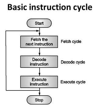 The time required to fetch an instruction and necessary data from memory and to execute it, is called an instruction cycle. Or the total time required to execute an instruction is given by:

Where,

Timing Diagram for Instruction Cycle

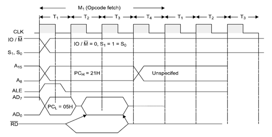
The whole operation of fetching an opcode takes three clock cycles. A slow memory may take more time.
If the operand is reside the general purpose registers, execution is immediately performed. The time taken in decoding and execution of an instruction is one clock cycle.
In some situations, an execute cycle may involve one or more read or write cycles or both.
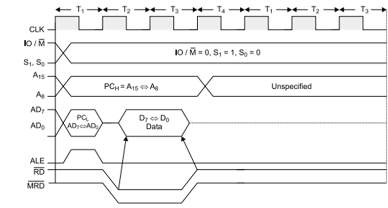
Read Cycle: If an instruction contains data or operand address which are in the memory, the CPU has to perform some read operations to get the desired data. In case of a read cycle the instruction received from the memory are data or operand address instead of an opcode.
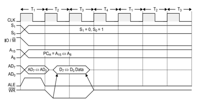
Write Cycle: In write cycle data are sent from the CPU to the memory or an output device.
One sub-division of an operation performed in one clock cycle is called a state or T-state. In short, one clock cycle of the system clock is referred to as a state.
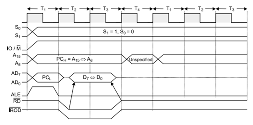
RD (low active): If it is high or 1, then no data is read by the microprocessor. If signal is low or 0, then data is read by the microprocessor.
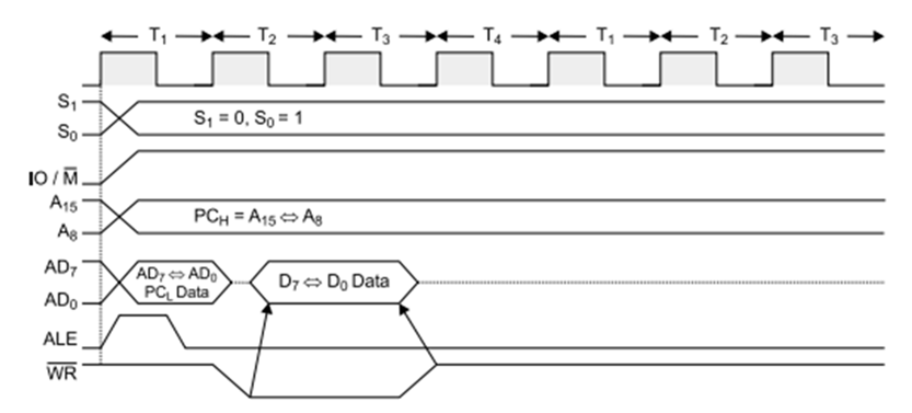
WR (low active): If it is high or 1, then no data is written by the microprocessor. If signal is low or 0, then data is written by the microprocessor.
IO/M (low active): A high or 1 on this signal indicates I/O operation while a low or 0 indicates memory operation.
S0, S1: S0 and S1 Indicate the type of machine cycle in progress.
The below table, shows the status of different control signal for different operation:

Instruction Cycle
 The time required to fetch an instruction and necessary data from memory and to execute it, is called an instruction cycle. Or the total time required to execute an instruction is given by:
Where,
Timing Diagram for Instruction Cycle

- Fetch the instruction (Fetch Cycle)
The whole operation of fetching an opcode takes three clock cycles. A slow memory may take more time.
- Decode the instruction (Decode Cycle)
- Execute the Instruction (Execute Cycle)
If the operand is reside the general purpose registers, execution is immediately performed. The time taken in decoding and execution of an instruction is one clock cycle.
In some situations, an execute cycle may involve one or more read or write cycles or both.
Read Cycle: If an instruction contains data or operand address which are in the memory, the CPU has to perform some read operations to get the desired data. In case of a read cycle the instruction received from the memory are data or operand address instead of an opcode.
Write Cycle: In write cycle data are sent from the CPU to the memory or an output device.
- Machine Cycle and State
One sub-division of an operation performed in one clock cycle is called a state or T-state. In short, one clock cycle of the system clock is referred to as a state.
Timing Diagram
The necessary steps carried out in a machine cycle can be represented graphically. Such a graphical representation is called timing diagram. The timing diagram for opcode fetch, memory read, memory write, I/O read and I/O write will be discussed below:- Timing Diagram for Opcode Fetch Cycle:

- Timing Diagram for Memory Read

- Timing Diagram for Memory Write

- Timing Diagram for I/O Read

- Timing Diagram for I/O Write

In the above diagrams, the basic used parameters are:
ALE: ALE indicates the availability of a valid address on the multiplexed address/data lines. When it is high or 1, then it acts as an address bus and when low or 0, then it acts as a data bus.RD (low active): If it is high or 1, then no data is read by the microprocessor. If signal is low or 0, then data is read by the microprocessor.
WR (low active): If it is high or 1, then no data is written by the microprocessor. If signal is low or 0, then data is written by the microprocessor.
IO/M (low active): A high or 1 on this signal indicates I/O operation while a low or 0 indicates memory operation.
S0, S1: S0 and S1 Indicate the type of machine cycle in progress.
The below table, shows the status of different control signal for different operation:


0 Comments