
SKYSPIN
Microprocessor - 8086 Pin Configuration
8086 was the first 16-bit microprocessor available in 40-pin DIP
(Dual Inline Package) chip. Let us now discuss in detail the pin
configuration of a 8086 Microprocessor.
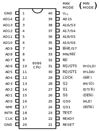
8086 Pin Diagram
Here is the pin diagram of 8086 microprocessor −
- The description of the pins of 8086 is as follows:
- AD0-AD15 (Address Data Bus): Bidirectional address/data lines. These are low order address bus. They are multiplexed with data.
- A16 - A19 (Output): High order address lines. These are multiplexed with status signals.
- A16/S3, A17/S4: A16 and A17 are multiplexed with segment identifier signals S3 and S4.
- A18/S5: A18 is multiplexed with interrupt status S5.
- A19/S6: A19 is multiplexed with status signal S6.
- BHE/S7 (Output): Bus High Enable/Status. During T1, it is low. It enables the data onto the most significant half of data bus, D8-D15. 8-bit device connected to upper half of the data bus use BHE signal. It is multiplexed with status signal S7. S7 signal is available during T3 and T4.
- RD (Read): For read operation. It is an output signal. It is active when LOW.
- Ready (Input): The addressed memory or I/O sends acknowledgment through this pin. When HIGH, it denotes that the peripheral is ready to transfer data.
- RESET (Input): System reset. The signal is active HIGH.
- CLK (input): Clock 5, 8 or 10 MHz.
- INTR: Interrupt Request.
- NMI (Input): Non-maskable interrupt request.
- TEST (Input): Wait for test control. When LOW the microprocessor continues execution otherwise waits.
- VCC: Power supply +5V dc.
- GND: Ground.


0 Comments