
SKYSPIN
UNIT-4 (TRENDS IN MICROPROCESSOR TECHNOLOGY)
Microprocessor - 8086 Overview
8086 Microprocessor is an enhanced version of 8085Microprocessor that
was designed by Intel in 1976. It is a 16-bit Microprocessor having 20
address lines and16 data lines that provides up to 1MB storage. It
consists of powerful instruction set, which provides operations like
multiplication and division easily.
It supports two modes of operation, i.e. Maximum mode and Minimum
mode. Maximum mode is suitable for system having multiple processors and
Minimum mode is suitable for system having a single processor.
Features of 8086
The most prominent features of a 8086 microprocessor are as follows −
- It has an instruction queue, which is capable of storing six instruction bytes from the memory resulting in faster processing.
- It was the first 16-bit processor having 16-bit ALU, 16-bit registers, internal data bus, and 16-bit external data bus resulting in faster processing.
- It is available in 3 versions based on the frequency of operation −
- 8086 → 5MHz
- 8086-2 → 8MHz
- (c)8086-1 → 10 MHz
- It uses two stages of pipelining, i.e. Fetch Stage and Execute Stage, which improves performance.
- Fetch stage can prefetch up to 6 bytes of instructions and stores them in the queue.
- Execute stage executes these instructions.
- It has 256 vectored interrupts.
- It consists of 29,000 transistors.
Comparison between 8085 & 8086 Microprocessor
- Size − 8085 is 8-bit microprocessor, whereas 8086 is 16-bit microprocessor.
- Address Bus − 8085 has 16-bit address bus while 8086 has 20-bit address bus.
- Memory − 8085 can access up to 64Kb, whereas 8086 can access up to 1 Mb of memory.
- Instruction − 8085 doesn’t have an instruction queue, whereas 8086 has an instruction queue.
- Pipelining − 8085 doesn’t support a pipelined architecture while 8086 supports a pipelined architecture.
- I/O − 8085 can address 2^8 = 256 I/O's, whereas 8086 can access 2^16 = 65,536 I/O's.
- Cost − The cost of 8085 is low whereas that of 8086 is high.
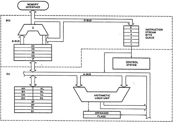
Architecture of 8086
The following diagram depicts the architecture of a 8086 Microprocessor −
Memory segmentation:
- To increase execution speed and fetching speed, 8086 segments the memory.
- It’s 20 bit address bus can address 1MB of memory, it segments it into 4 64kB segments.
- 8086 works only with four 64KB segments within the whole 1MB memory.
Functional units of 8086
8086 contains two independent functional units: a Bus Interface Unit (BIU) and an Execution Unit (EU).
Bus Interface Unit (BIU)
The segment registers, instruction pointer and 6-byte instruction queue are associated with the bus interface unit (BIU).
The BIU:
- Handles transfer of data and addresses,
- Fetches instruction codes, stores fetched instruction codes in first-in-first-out register set called a queue,
- Reads data from memory and I/O devices,
- Writes data to memory and I/O devices,
- It relocates addresses of operands since it gets un-relocated operand addresses from EU. The EU tells the BIU from where to fetch instructions or where to read data.
It has the following functional parts:
- Instruction Queue: When EU executes instructions, the BIU gets 6-bytes of the next instruction and stores them in the instruction queue and this process is known as instruction pre fetch. This process increases the speed of the processor.
- Segment Registers: A segment register contains the
addresses of instructions and data in memory which are used by the
processor to access memory locations. It points to the starting address
of a memory segment currently being used.
There are 4 segment registers in 8086 as given below:- Code Segment Register (CS): Code segment of the memory holds instruction codes of a program.
- Data Segment Register (DS): The data, variables and constants given in the program are held in the data segment of the memory.
- Stack Segment Register (SS): Stack segment holds addresses and data of subroutines. It also holds the contents of registers and memory locations given in PUSH instruction.
- Extra Segment Register (ES): Extra segment holds the destination addresses of some data of certain string instructions.
- Instruction Pointer (IP): The instruction pointer in the 8086 microprocessor acts as a program counter. It indicates to the address of the next instruction to be executed.
Execution Unit (EU)
- The EU receives opcode of an instruction from the queue, decodes it and then executes it. While Execution, unit decodes or executes an instruction, then the BIU fetches instruction codes from the memory and stores them in the queue.
- The BIU and EU operate in parallel independently. This makes processing faster.
- General purpose registers, stack pointer, base pointer and index registers, ALU, flag registers (FLAGS), instruction decoder and timing and control unit constitute execution unit (EU). Let's discuss them:
OR
Execution unit gives instructions to BIU stating from where to fetch
the data and then decode and execute those instructions. Its function is
to control operations on data using the instruction decoder & ALU.
EU has no direct connection with system buses as shown in the above
figure, it performs operations over data through BIU.
Let us now discuss the functional parts of 8086 microprocessors.
ALU
It handles all arithmetic and logical operations, like +, −, ×, /, OR, AND, NOT operations.
Flag Register
It is a 16-bit register that behaves like a flip-flop, i.e. it
changes its status according to the result stored in the accumulator. It
has 9 flags and they are divided into 2 groups − Conditional Flags and
Control Flags.
Conditional Flags
It represents the result of the last arithmetic or logical instruction executed. Following is the list of conditional flags −
- Carry flag − This flag indicates an overflow condition for arithmetic operations.
- Auxiliary flag − When an operation is performed at ALU, it results in a carry/barrow from lower nibble (i.e. D0 – D3) to upper nibble (i.e. D4 – D7), then this flag is set, i.e. carry given by D3 bit to D4 is AF flag. The processor uses this flag to perform binary to BCD conversion.
- Parity flag − This flag is used to indicate the parity of the result, i.e. when the lower order 8-bits of the result contains even number of 1’s, then the Parity Flag is set. For odd number of 1’s, the Parity Flag is reset.
- Zero flag − This flag is set to 1 when the result of arithmetic or logical operation is zero else it is set to 0.
- Sign flag − This flag holds the sign of the result, i.e. when the result of the operation is negative, then the sign flag is set to 1 else set to 0.
- Overflow flag − This flag represents the result when the system capacity is exceeded.
Control Flags
Control flags controls the operations of the execution unit. Following is the list of control flags −
- Trap flag − It is used for single step control and allows the user to execute one instruction at a time for debugging. If it is set, then the program can be run in a single step mode.
- Interrupt flag − It is an interrupt enable/disable flag, i.e. used to allow/prohibit the interruption of a program. It is set to 1 for interrupt enabled condition and set to 0 for interrupt disabled condition.
- Direction flag − It is used in string operation. As the name suggests when it is set then string bytes are accessed from the higher memory address to the lower memory address and vice-a-versa.
General purpose register
There are 8 general purpose registers, i.e., AH, AL, BH, BL, CH, CL,
DH, and DL. These registers can be used individually to store 8-bit data
and can be used in pairs to store 16bit data. The valid register pairs
are AH and AL, BH and BL, CH and CL, and DH and DL. It is referred to
the AX, BX, CX, and DX respectively.
- AX register − It is also known as accumulator register. It is used to store operands for arithmetic operations.
- BX register − It is used as a base register. It is used to store the starting base address of the memory area within the data segment.
- CX register − It is referred to as counter. It is used in loop instruction to store the loop counter.
- DX register − This register is used to hold I/O port address for I/O instruction.
Stack pointer register
It is a 16-bit register, which holds the address from the start of
the segment to the memory location, where a word was most recently
stored on the stack.
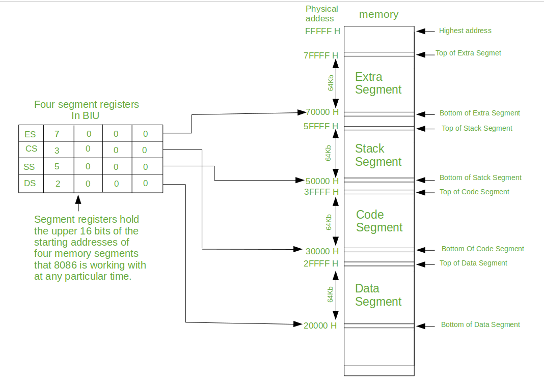
Memory Segmentation in 8086 Microprocessor
Segmentation is the process in which the main memory of the
computer is logically divided into different segments and each segment
has its own base address. It is basically used to enhance the speed of
execution of the computer system, so that the processor is able to fetch
and execute the data from the memory easily and fast.
Need for Segmentation –
The Bus Interface Unit (BIU) contains four 16 bit special purpose registers (mentioned below) called as Segment Registers.
- Code segment register (CS): is used for addressing memory location in the code segment of the memory, where the executable program is stored.
- Data segment register (DS): points to the data segment of the memory where the data is stored.
- Extra Segment Register (ES): also refers to a segment in the memory which is another data segment in the memory.
- Stack Segment Register (SS): is used for addressing stack segment of the memory. The stack segment is that segment of memory which is used to store stack data.
The number of address lines in 8086 is 20, 8086 BIU will send 20bit
address, so as to access one of the 1MB memory locations. The four
segment registers actually contain the upper 16 bits of the starting
addresses of the four memory segments of 64 KB each with which the 8086
is working at that instant of time. A segment is a logical unit of
memory that may be up to 64 kilobytes long. Each segment is made up of
contiguous memory locations. It is an independent, separately
addressable unit. Starting address will always be changing. It will not
be fixed.
Note that the 8086 does not work the whole 1MB memory at any given
time. However, it works only with four 64KB segments within the whole
1MB memory.
Below is the one way of positioning four 64 kilobyte segments within the 1M byte memory space of an 8086.
Types Of Segmentation –
- Overlapping Segment – A segment starts at a particular address and its maximum size can go up to 64kilobytes. But if another segment starts along with this 64kilobytes location of the first segment, then the two are said to be Overlapping Segment.
- Non-Overlapped Segment – A segment starts at a particular address and its maximum size can go up to 64kilobytes. But if another segment starts before this 64kilobytes location of the first segment, then the two segments are said to be Non-Overlapped Segment.
Rules of Segmentation Segmentation process follows some rules as follows:

Advantages of the Segmentation The main advantages of segmentation are as follows:
- It provides a powerful memory management mechanism.
- Data related or stack related operations can be performed in different segments.
- Code related operation can be done in separate code segments.
- It allows to processes to easily share data.
- It allows to extend the address ability of the processor, i.e. segmentation allows the use of 16 bit registers to give an addressing capability of 1 Megabytes. Without segmentation, it would require 20 bit registers.
- It is possible to enhance the memory size of code data or stack segments beyond 64 KB by allotting more than one segment for each area.
- The starting address of a segment should be such that it can be evenly divided by 16.
- Minimum size of a segment can be 16 bytes and the maximum can be 64 kB.
Addressing modes in 8086 microprocessor
The way for which an operand is specified for an instruction in the
accumulator, in a general purpose register or in memory location, is
called addressing mode.
The 8086 microprocessors have 8 addressing modes. Two addressing
modes have been provided for instructions which operate on register or
immediate data.
These two addressing modes are:
Register Addressing: In register addressing, the operand is placed in one of the 16-bit or 8-bit general purpose registers.
Example
- MOV AX, CX
- ADD AL, BL
- ADD CX, DX
Immediate Addressing: In immediate addressing, the operand is specified in the instruction itself.
Example
- MOV AL, 35H
- MOV BX, 0301H
- MOV [0401], 3598H
- ADD AX, 4836H
The remaining 6 addressing modes specify the location of an operand which is placed in a memory.
These 6 addressing modes are:
Direct Addressing: In direct addressing mode, the operand?s offset is given in the instruction as an 8-bit or 16-bit displacement element.
Example
- ADD AL, [0301]
The instruction adds the content of the offset address 0301 to AL.
the operand is placed at the given offset (0301) within the data segment
DS.
Register Indirect Addressing: The operand's offset is placed in any one of the registers BX, BP, SI or DI as specified in the instruction.
Example
- MOV AX, [BX]
It moves the contents of memory locations addressed by the register BX to the register AX.
Based Addressing: The operand's offset is the sum of
an 8-bit or 16-bit displacement and the contents of the base register
BX or BP. BX is used as base register for data segment, and the BP is
used as a base register for stack segment.
Effective address (Offset) = [BX + 8-bit or 16-bit displacement].
Example
- MOV AL, [BX+05]; an example of 8-bit displacement.
- MOV AL, [BX + 1346H]; example of 16-bit displacement.
Indexed Addressing: The offset of an operand is the sum of the content of an index register SI or DI and an 8-bit or 16-bit displacement.
Offset (Effective Address) = [SI or DI + 8-bit or 16-bit displacement]
Example
- MOV AX, [SI + 05]; 8-bit displacement.
- MOV AX, [SI + 1528H]; 16-bit displacement.
Based Indexed Addressing: The offset of operand is the sum of the content of a base register BX or BP and an index register SI or DI.
Effective Address (Offset) = [BX or BP] + [SI or DI]
Here, BX is used for a base register for data segment, and BP is used as a base register for stack segment.
Example
- ADD AX, [BX + SI]
- MOV CX, [BX + SI]
Based Indexed with Displacement: In this mode of addressing, the operand's offset is given by:
Effective Address (Offset) = [BX or BP] + [SI or DI] + 8-bit or 16-bit displacement
Example
- MOV AX, [BX + SI + 05]; 8-bit displacement
- MOV AX, [BX + SI + 1235H]; 16-bit displacement
Microprocessor - 8086 Pin Configuration
8086 was the first 16-bit microprocessor available in 40-pin DIP
(Dual Inline Package) chip. Let us now discuss in detail the pin
configuration of a 8086 Microprocessor.
8086 Pin Diagram
Here is the pin diagram of 8086 microprocessor −
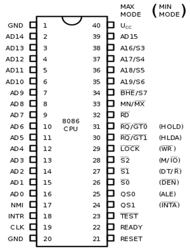
- The description of the pins of 8086 is as follows:
- AD0-AD15 (Address Data Bus): Bidirectional address/data lines. These are low order address bus. They are multiplexed with data.
- A16 - A19 (Output): High order address lines. These are multiplexed with status signals.
- A16/S3, A17/S4: A16 and A17 are multiplexed with segment identifier signals S3 and S4.
- A18/S5: A18 is multiplexed with interrupt status S5.
- A19/S6: A19 is multiplexed with status signal S6.
- BHE/S7 (Output): Bus High Enable/Status. During T1, it is low. It enables the data onto the most significant half of data bus, D8-D15. 8-bit device connected to upper half of the data bus use BHE signal. It is multiplexed with status signal S7. S7 signal is available during T3 and T4.
- RD (Read): For read operation. It is an output signal. It is active when LOW.
- Ready (Input): The addressed memory or I/O sends acknowledgment through this pin. When HIGH, it denotes that the peripheral is ready to transfer data.
- RESET (Input): System reset. The signal is active HIGH.
- CLK (input): Clock 5, 8 or 10 MHz.
- INTR: Interrupt Request.
- NMI (Input): Non-maskable interrupt request.
- TEST (Input): Wait for test control. When LOW the microprocessor continues execution otherwise waits.
- VCC: Power supply +5V dc.
- GND: Ground.
Operating Modes of 8086
There are two operating modes of operation for Intel 8086, namely the minimum mode and the maximum mode.
When only one 8086 CPU is to be used in a microprocessor system, the 8086 is used in the Minimum mode of operation.
In a multiprocessor system 8086 operates in the Maximum mode.
Pin Description for Minimum Mode
In this minimum mode of operation, the pin MN/MX is connected to 5V D.C. supply i.e. MN/MX = VCC.
The description about the pins from 24 to 31 for the minimum mode is as follows: - INTA (Output): Pin number 24 interrupts acknowledgement. On receiving interrupt signal, the processor issues an interrupt acknowledgment signal. It is active LOW.
- ALE (Output): Pin no. 25. Address latch enable. It goes HIGH during T1. The microprocessor 8086 sends this signal to latch the address into the Intel 8282/8283 latch.
- DEN (Output): Pin no. 26. Data Enable. When Intel 8287/8286 octal bus transceiver is used this signal. It is active LOW.
- DT/R (output): Pin No. 27 data Transmit/Receives. When Intel 8287/8286 octal bus transceiver is used this signal controls the direction of data flow through the transceiver. When it is HIGH, data is sent out. When it is LOW, data is received.
- M/IO (Output): Pin no. 28, Memory or I/O access. When this signal is HIGH, the CPU wants to access memory. When this signal is LOW, the CPU wants to access I/O device.
- WR (Output): Pin no. 29, Write. When this signal is LOW, the CPU performs memory or I/O write operation.
- HLDA (Output): Pin no. 30, Hold Acknowledgment. It is sent by the processor when it receives HOLD signal. It is active HIGH signal. When HOLD is removed HLDA goes LOW.
- HOLD (Input): Pin no. 31, Hold. When another device in microcomputer system wants to use the address and data bus, it sends HOLD request to CPU through this pin. It is an active HIGH signal.
Pin Description for Maximum Mode
In the maximum mode of operation, the pin MN/¯MX is made LOW. It is
grounded. The description about the pins from 24 to 31 is as follows:
- QS1, QS0 (Output): Pin numbers 24, 25, Instruction Queue Status. Logics are given below:
-

- S0, S1, S2 (Output): Pin numbers 26, 27, 28 Status Signals. These signals are connected to the bus controller of Intel 8288. This bus controller generates memory and I/O access control signals. Logics for status signal are given below:
- LOCK (Output): Pin no. 29. It is an active LOW signal. When this signal is LOW, all interrupts are masked and no HOLD request is granted. In a multiprocessor system all other processors are informed through this signal that they should not ask the CPU for relinquishing the bus control.
RG/GT1, RQ/GT0
(Bidirectional): Pin numbers 30, 31, Local Bus Priority Control. Other
processors ask the CPU by these lines to release the local bus.
In the maximum mode of operation signals WR, ALE, DEN, DT/R etc. are not available directly from the processor. These signals are available from the controller 8288.
8087 Numeric Data Processor
8087 numeric data processor is also known as Math co-processor, Numeric processor extension and Floating point unit. It was the first math coprocessor designed by Intel to pair with 8086/8088 resulting in easier and faster calculation.
Once the instructions are identified by the 8086/8088 processor, then
it is allotted to the 8087 co-processor for further execution.
The data types supported by 8087 are −
- Binary Integers
- Packed decimal numbers
- Real numbers
- Temporary real format
The most prominent features of 8087 numeric data processor are as follows −
- It supports data of type integer, float, and real types ranging from 2-10 bytes.
- The processing speed is so high that it can calculate multiplication of two 64-bits real numbers in ~27 µs and can also calculate square-root in ~35 µs.
- It follows IEEE floating point standards.
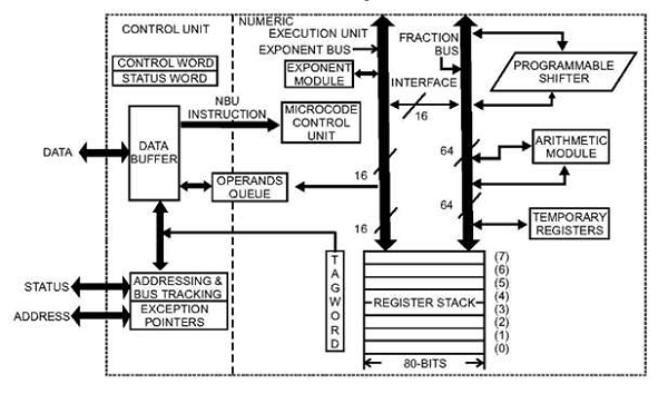
8087 Architecture
8087 Architecture is divided into two groups, i.e., Control Unit (CU) and Numeric Extension Unit (NEU).
- The control unit handles all the communication between the processor and the memory such as it receives and decodes instructions, reads and writes memory operands, maintains parallel queue, etc. All the coprocessor instructions are ESC instructions, i.e., they start with ‘F’, the coprocessor only executes the ESC instructions while other instructions are executed by the microprocessor.
- The numeric extension unit handles all the numeric processor instructions like arithmetic, logical, transcendental, and data transfer instructions. It has 8 register stack, which holds the operands for instructions and their results.
The architecture of 8087 coprocessor is as follows −
8087 Pin Description
Let us first take a look at the pin diagram of 8087 −
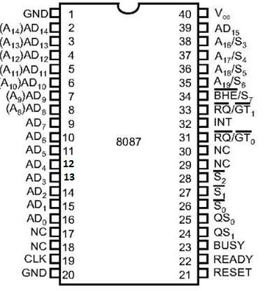 The following list provides the Pin Description of 8087 −
- AD0 – AD15 − These are the time multiplexed address/data lines, which carry addresses during the first clock cycle and data from the second clock cycle onwards.
- A19 / S6 – A16/S − These lines are the time multiplexed address/status lines. It functions in a similar way to the corresponding pins of 8086. The S6, S4 and S3 are permanently high, while the S5 is permanently low.
- $\overline{BHE}$/S7 − During the first clock cycle, the $\overline{BHE}$/S7 is used to enable data on to the higher byte of the 8086 data bus and after that works as status line S7.
- QS1, QS0 − These are queue status
input signals which provides the status of instruction queue, their
conditions as shown in the following table −

- INT − It is an interrupt signal, which changes to high when an unmasked exception has been received during the execution.
- BUSY − It is an output signal, when it is high it indicates a busy state to the CPU.
- READY − It is an input signal used to inform the coprocessor whether the bus is ready to receive data or not.
- RESET − It is an input signal used to reject the internal activities of the coprocessor and prepare it for further execution whenever required by the CPU.
- CLK − The CLK input provides the basic timings for the processor operation.
- VCC − It is a power supply signal, which requires +5V supply for the operation of the circuit.
- S0, S1, S2 − These are the status signals that provide the status of the operation which is used by the Bus Controller 8087 to generate memory and I/O control signals. These signals are active during the fourth clock cycle.
 RQ/GT1 & RQ/GT0 − These are the Request/Grant signals used by the 8087 processors to gain control of the bus from the host processor 8086/8088 for operand transfers.
Coprocessor Configuration
A Coprocessor is a specially designed circuit on microprocessor chip
which can perform the same task very quickly, which the microprocessor
performs. It reduces the work load of the main processor. The
coprocessor shares the same memory, IO system, bus, control logic and
clock generator. The coprocessor handles specialized tasks like
mathematical calculations, graphical display on screen, etc.
The 8086 and 8088 can perform most of the operations but their
instruction set is not able to perform complex mathematical operations,
so in these cases the microprocessor requires the math coprocessor like
Intel 8087 math coprocessor, which can easily perform these operations
very quickly.
Block Diagram of Coprocessor Configuration
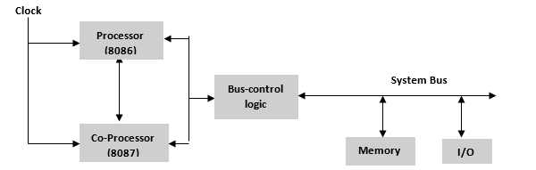
How is the coprocessor and the processor connected?
- The coprocessor and the processor is connected via TEST, RQ-/GT- and QS0 & QS1 signals.
- The TEST signal is connected to BUSY pin of coprocessor and the remaining 3 pins are connected to the coprocessor’s 3 pins of the same name.
- TEST signal takes care of the coprocessor’s activity, i.e. the coprocessor is busy or idle.
- The RT-/GT-is used for bus arbitration.
- The coprocessor uses QS0 & QS1 to track the status of the queue of the host processor.


0 Comments